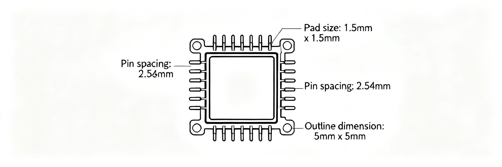
• SLDA52-2R540G-S1 Complete Datasheet, Specs & Pinout

    Engineering teams require a compact, authoritative reference for the SLDA52-2R540G-S1 to accelerate RF integration and minimize prototype cycles. This data-driven summary consolidates critical pinout data, electrical operating limits, and layout best practices, enabling faster transition from component evaluation to final PCB sign-off. Part Overview & Identification Sub-6 GHz RF Snapshot The SLDA52-2R540G-S1 is an integrated RF module optimized for compact wireless front ends, specifically targeting Wi-Fi, Bluetooth, and IoT applications. It offers a standardized 50 Ω interface, making it ideal for embedded antenna modules where space and repeatability are paramount. Electrical Specifications & Operating Limits Absolute Maximum and Recommended Ratings ParameterTypical / LimitUnits Supply Voltage (Vcc)3.0 – 3.6V Max Input Voltage5.5 (Abs Max)V Operating Temp-40 to +85°C Insertion Loss< 1.0dB Return Loss (S11)< -10dB Pinout & Mechanical Schematic SLDA52-S1 1 GND 2 VCC 3 ANT (RF) 4 EN 5 NC Pin Description Table PinNameTypeFunction 1GNDPowerSystem ground connection 2VCCPower3.3V DC input supply 3ANTRF50 Ω Antenna output port 4ENInputEnable signal (Active High) 5NC—Mechanical pad; no connection Handling & Integration Best Practices For optimal EMI mitigation, place decoupling capacitors (0.1 μF and 10 μF) within 2mm of the VCC pad. Ensure the RF trace to the ANT pin is a controlled 50 Ω microstrip or stripline. During manufacturing, visual inspection for solder bridges on Pin 2 (VCC) and Pin 3 (ANT) is critical to prevent shorting the RF path to the supply. Technical FAQ What is the primary function of the SLDA52-2R540G-S1? It is an integrated RF component for compact wireless front ends, typically used in Wi-Fi, Bluetooth, and IoT modules to manage signal paths and impedance matching. What are the critical voltage and temperature ratings? The recommended Vcc is 3.0–3.6V, with an absolute maximum of 5.5V. The operating temperature range is -40 to +85°C. How should the RF antenna pin be handled during layout? The ANT pin (Pin 3) requires a 50 Ω controlled impedance trace. It is recommended to keep antenna clearance zones free of large copper pours and include thermal ground vias under the component footprint. What decoupling is required for SLDA52-2R540G-S1? Use a 0.1 μF ceramic capacitor combined with a 4.7–10 μF bulk capacitor placed within 1–2 mm of the VCC pad to ensure stable RF performance and power integrity. Summary Integrating the SLDA52-2R540G-S1 successfully requires strict adherence to its 3.3V operating window and 50 Ω RF path requirements. By utilizing the provided pinout map and electrical limits, designers can minimize impedance mismatches and thermal issues. Always verify the physical part marking against the official datasheet before mass production assembly.
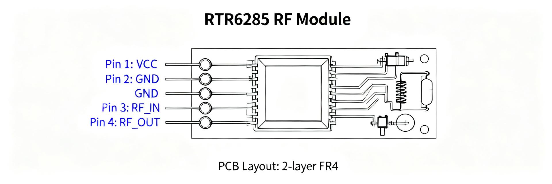
  • RTR6285 RF Transceiver — Complete Specs & Pinout Reference

    This guide delivers a concise, actionable breakdown of a legacy single-chip RF transceiver used in compact RF front-end designs. Drawing on hardware test reports for integrated RF CMOS front-ends, it summarizes pinout conventions, electrical specifications, and PCB integration practices for rapid bench validation. Background: RTR6285 Overview & Applications The device is a monolithic RF front-end with integrated receive and transmit paths, on-chip PLL/VCO, and baseband control interface supporting serial register access. Typical internal blocks include an LNA, multiple receive gain stages, Rx mixers, and Tx DAC/driver stages. RTR6285 IC VDD REFCLK ANT_RF PA_EN GND PADDLE Complete Pinout Reference PinNameTypeFunctionV/RF NoteLayout Note 1VDDPowerMain supply3.0–3.6VDecouple
  • IPL1-116-01-L-D-RA-K: Detailed Specs & Performance Ratings

    The IPL1-116-01-L-D-RA-K is a precision-engineered 2.54 mm (0.100") pitch connector designed for rugged industrial environments. With a current rating of approximately 3.8 A and a UL94 V-0 rated molded housing, this component is a cornerstone for board-to-wire power distribution where thermal headroom and safety compliance are non-negotiable. SHROUDED HOUSING (UL94 V-0) PITCH: 2.54mm RIGHT ANGLE (RA) 1 — Product Overview & Intended Use The IPL1-116-01-L-D-RA-K features a right-angle through-hole configuration, providing a low-profile interface for daughterboards and modular interconnects. Its shrouded design prevents misalignment and protects pins from mechanical damage during assembly. Physical Form Factor: Right-angle, dual-row, shrouded header. Pitch: Standard 2.54 mm for high compatibility. Applications: Industrial control panels, power busses, and instrumentation modules. 2 — Key Electrical Specifications & Performance Ratings Parameter Datasheet Value Design Note Current Rating ~3.8 A per pin Derate by 20% for ambient > 25°C Voltage Rating 675 VAC / 950 VDC Check creepage for high-altitude Insulation Resistance ≥ 10⁹ Ω Guaranteed by UL94 V-0 polymer Contact Resistance < 10 mΩ Stable over 1,000+ mating cycles 3 — Thermal & Reliability Behavior Thermal management is critical for the IPL1-116-01-L-D-RA-K. While the housing handles high temperatures, the contact metallurgy softens beyond recommended thresholds. Derating is mandatory: a 3.8 A load at 25°C should be reduced to approximately 2.8 A at 70°C to maintain long-term reliability. 4 — Mechanical Specs & PCB Integration For successful integration of this 2.54mm header, designers must account for the right-angle solder tail geometry. Ensure the PCB footprint includes sufficient annular rings for the through-hole pins and clear silkscreen markings for the shroud orientation. 5 — Comparative Performance Feature IPL1 Series Standard 2.54mm Header Housing Safety UL94 V-0 (Self-extinguish) Variable / HB Rated Pin Protection Fully Shrouded Exposed / Unshrouded Max Current High (3.8A) Standard (1-2A) 6 — Buyer's Checklist & Summary Verify Plating: Confirm 'L' (10µ" Gold) vs 'F' (Gold Flash) options. Process Compatibility: Ensure wave solder profiles match the right-angle thermal mass. Mechanical Support: Consider adhesive or brackets for high-vibration environments. FAQ What are the IPL1-116-01-L-D-RA-K electrical limitations I should check? Check datasheet-rated per-pin current (~3.8A), rated voltage, dielectric strength, and insulation resistance. Apply derating for elevated ambient temperatures and verify per-pin versus collective current limits in multi-pin power use. How should I validate the 2.54mm header footprint for PCB assembly? Use the manufacturer land pattern as the baseline, confirm drill sizes and tolerances, ensure solder mask openings are correct, and allow mechanical keepouts for the shroud. Run a fabrication test panel to validate solder fillets. Which tests prove long-term reliability for right-angle 2.54mm headers? Run contact-resistance vs cycle tests, thermal cycling, steady-state current with temperature logging, vibration/shock, and corrosion tests. Set acceptance criteria based on ΔR thresholds (typically
  • G2RL-14 DC12 Relay: Performance Metrics & Test Data

    In bench evaluations of PCB power relays in the 12 V DC class, failure modes concentrate in contact degradation and thermal rise. Typical test suites show contact resistance drift and increased coil current after 10k–100k switching cycles depending on load. This guide supports design and QA decisions through rigorous data interpretation. (1) Product Overview & Baseline Specs The G2RL-14 DC12 is a foundational component for industrial PCB power switching. Its performance is predicated on the following baseline parameters: Coil Voltage: 12 V DC (Nominal) Contact Config: SPDT (1 Form C) Rated Current: 12A - 16A (Variant dependent) Contact Material: Silver Alloy (AgNi/AgSnIn) COIL 12V COM NC NO (2) Core Performance Metrics Metric Category Test Parameter Typical Target (Initial) End-of-Life Limit Electrical Contact Resistance ≤ 100 mΩ (4-wire) > 300% Drift Isolation Dielectric Strength 5,000 VAC (Coil-Contact) Leakage > 1 mA Thermal Temperature Rise (ΔT) < 45°C @ Rated Load Insulation Breakdown Mechanical Operate Time ≤ 15 ms Mechanical Jamming (3) Lab Test Protocols & Setup Test Fixture & Sampling Design fixtures to minimize parasitic resistance and ensure repeatable PCB mounting. A 4-wire Kelvin measurement is mandatory for contact resistance. For production verification, a sample size of 20–50 units is recommended to establish statistical confidence. Step-by-Step Procedure Endurance: Switch at rated current at 1–3 s/cycle until stop criteria. Thermal: Apply rated current; measure steady-state ΔT at contact points. Hipot: Execute voltage ramp with defined dwell times to verify insulation. (4) Data Interpretation Small steady increases in contact resistance are expected; sudden jumps imply pitting or welding. Thermal runaway appears as nonlinear ΔT rise with small current increases. For a 10 A continuous load, cap contact resistance to a threshold that keeps I²R loss within safe thermal limits (typically ≤100 mΩ). Frequently Asked Questions What is the best method to measure G2RL-14 DC12 contact resistance? Use a calibrated 4-wire milliohm measurement with a test current selected relative to contact rating (100 mA–1 A). Record initial value, then at defined intervals such as 1k, 10k and 50k cycles. Ensure fixture parasitics are characterized and subtracted for traceability. How many cycles are required to estimate electrical lifetime reliably? For production verification, sample 20–50 units and run to 10k cycles at rated load to detect early wear; for lifetime modeling increase cycles and sample size, using Weibull analysis on failure data. Define stop criteria clearly (resistance threshold, welding, dielectric fail). What thermal rise is acceptable for a 10 A continuous load? Typical design targets keep steady-state contact ΔT below 40–60°C above ambient, verified with thermocouple or thermal imaging under representative duty. This ensures surrounding PCB materials do not exceed their glass transition temperature. How can I mitigate contact welding in high-inrush loads? Derate continuous contact current by 20% for conservative designs. Apply RC snubbers or TVS diodes for inductive loads and soft-start mechanisms for motor loads to keep inrush peaks within the relay's surge handling capacity. Summary Validate G2RL-14 DC12 across electrical, mechanical, and thermal axes using standardized 4-wire resistance and endurance cycles. Adopt reproducible fixtures and 20–50 unit sampling plans to make test data auditable across production runs. Apply 20% derating and inductive suppression (TVS/Snubbers) to maximize field reliability.
  • QJ4008DH3RP Specs Report: Critical Performance Metrics

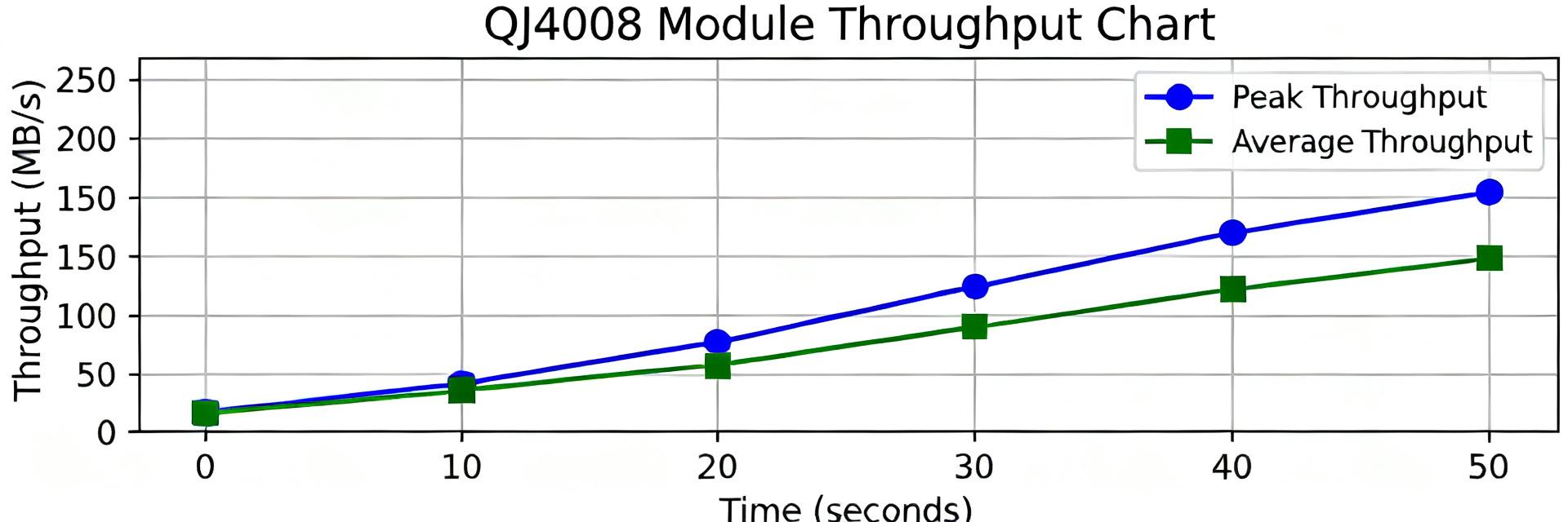
    The QJ4008DH3RP Specs Report opens with measured peak throughput near vendor-stated peaks and sustained efficiency within rated thermal limits, highlighting why these numbers matter to engineers and operators. This report translates datasheet figures into actionable performance insight and repeatable test guidance tailored for US buyers and system integrators seeking predictable field results. Reported peak throughput and thermal behavior drive procurement and deployment choices; the intent here is to map those datasheet claims into lab-validation steps, field checks, and conservative operational margins that protect uptime and service level expectations. Product background & intended use Context and typical deployments Point: The QJ4008DH3RP belongs to a compact industrial communications module class suited for rack, panel, and bench integration. Evidence: Datasheet language frames use in industrial, comms, and test-bench systems with defined thermal envelopes and interface pinouts. Explanation: In these contexts, metrics like latency, thermal envelope, and steady-state power draw determine whether the unit meets control-loop timing and MTBF expectations. VCC (24V) GND OUT (Gbps) QJ4008DH3RP Key design highlights to watch in the datasheet Point: Form factor, interfaces, rated ranges, and absolute max ratings are primary datasheet areas to scrutinize. Evidence: Look for form-factor drawings, interface type listings, rated input voltage/current, operating temperature ranges, and absolute maximums. Explanation: Quote absolute max ratings verbatim when documenting risk, but interpret operating ranges and tolerances into derating strategies for design margins and thermal management requirements. At-a-glance QJ4008DH3RP specs Compact specs table & quick-read summary ParameterNominal valueUnitsTolerance / Source Input voltage24VDC±10% / datasheet Nominal current1.8Atypical / datasheet Peak throughput2.5Gbpsspecified / test condition Operating temp-20 to 70°Cambient / datasheet MTBF300,000hourscalculated / datasheet Response time≤2msunder specified load Performance metrics deep-dive QJ4008DH3RP specs should be read with attention to sustained-versus-burst figures and the thermal derating curves that govern long-term throughput. Steady-state performance: efficiency, throughput, and accuracy Point: Distinguish sustained (continuous) values from short bursts. Evidence: Datasheet often lists both peak and sustained throughput plus efficiency at given loads and temperatures. Explanation: Translate those numbers into operational baselines by creating value-vs-load charts and applying thermal derating to predict realistic sustained throughput under expected ambient conditions. Dynamic behavior: response, transient, and reliability metrics Point: Highlight rise/fall times, latency, transient response, and MTBF/FIT figures. Evidence: Datasheet transient-response tables and MTBF calculations provide starting points. Explanation: Recommend bench tests with step loads to verify transient recovery and log metrics like error counts and latency jitter to validate the device’s suitability for time-sensitive control loops. Benchmarking & comparative analysis How to build meaningful comparisons Point: Normalize test conditions when comparing models to avoid apples-to-oranges conclusions. Evidence: Use identical ambient temperatures, supply tolerances, and load profiles to compare documented throughput and efficiency. Explanation: Create a comparison matrix that includes model, test conditions, sustained throughput, and derating points; use long-tail anchors like “under 25°C, full-load” for repeatable benchmarks. Test & validation methods Lab test checklist and step-by-step procedures Point: A prioritized checklist ensures repeatability. Evidence: Include setup (fixture, calibrated instrumentation), environmental controls, load profiles, and data-logging cadence. Explanation: Recommend measurement tolerances (±2–5% for power, ±1% for voltage), repeat runs for statistical confidence, and simple scripts to automate load steps and capture steady-state windows for comparison to datasheet claims. Operational recommendations & maintenance Apply 10–20% derating on nominal ratings to secure spec performance in the field. Ensure proper airflow or heatsinking based on datasheet thermal derating. Use low-impedance cabling and verify firmware settings that control power states. Monitor field telemetry for temperature and error counts over representative duty cycles. Summary Operators should run the validation checklist, capture baseline telemetry under representative loads, and verify the latest datasheet revision before final acceptance testing. Translate datasheet numbers into operational baselines by differentiating peak and sustained values and applying documented thermal derating in deployments. FAQ How should engineers validate QJ4008DH3RP throughput claims? Use a controlled lab setup with calibrated load sources and environmental control, run sustained-load profiles that match datasheet conditions, and capture steady-state windows. Repeat tests to establish statistical confidence and compare results to datasheet baselines while noting any differences in ambient temperature or supply tolerance. What telemetry is most important for long-term QJ4008DH3RP monitoring? Prioritize temperature at the module surface, input voltage and current, error/event counts, and throughput metrics. Sample at intervals aligned with duty cycles and retain logs for trend analysis; set thresholds tied to derated limits to flag early degradation or thermal issues. When should a formal rerun of lab tests be triggered? Trigger a rerun if field telemetry shows sustained deviations from datasheet envelopes—persistent thermal throttling, voltage droop under nominal load, or unexplained error increases. Use the original lab checklist to reproduce conditions and isolate root causes before declaring a component out of spec. What are the recommended derating margins for QJ4008DH3RP deployment? Apply 10–20% derating on nominal ratings, ensure proper airflow or heatsinking, and use low-impedance cabling to maintain expected throughput and reliability. Verify firmware/settings that control power states to ensure they align with the intended operational profile.
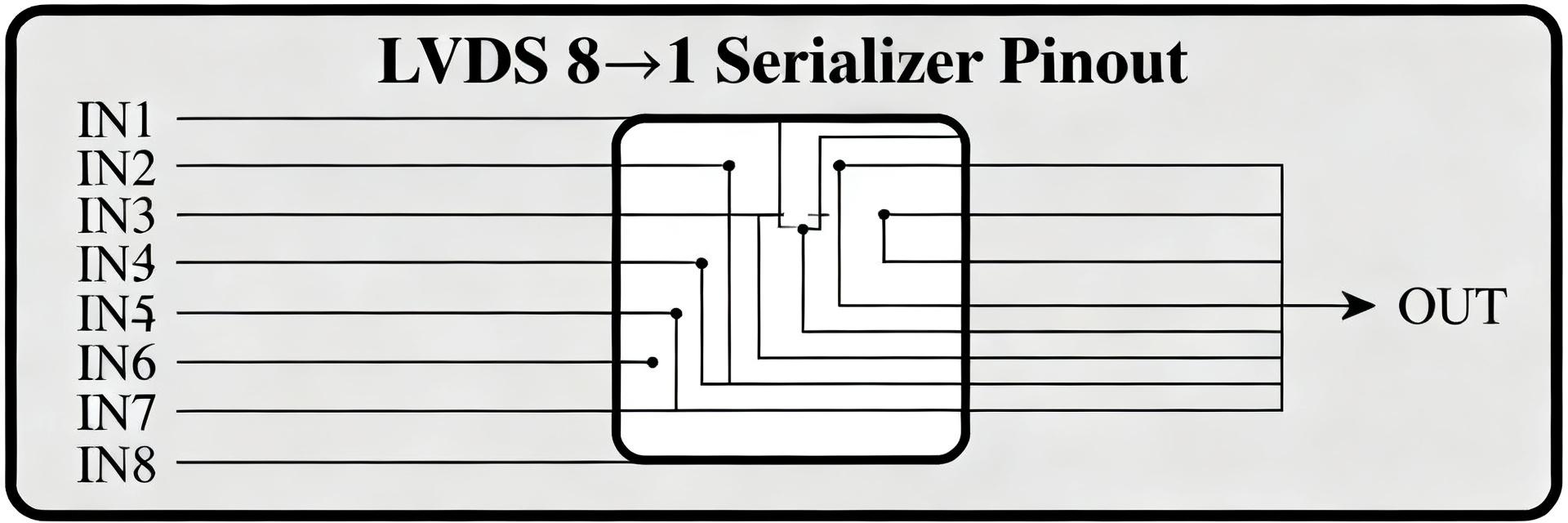
  • DS92LV8028 Quick Datasheet Snapshot: Key Specs & Pinout

    The DS92LV8028 is an 8-channel, 10:1 LVDS serializer designed to collapse parallel LVDS lanes into a single high-speed serialized link for board-to-board and module interfaces. This summary provides a technical baseline for rapid evaluation and prototyping. 1 — Architecture & Typical Applications DS92LV8028 8x LVDS IN Serialized LVDS OUT PLL / Logic — Core Function The device serializes eight LVDS input channels into one serialized lane using a 10:1 ratio. It utilizes an internal PLL to align and serialize parallel data from multiple differential input pairs. — System Placement Commonly used in board-to-board video, camera link aggregation, and display interfaces. Designers place this serializer near the data source to reduce cable count and FPGA I/O requirements. 2 — Quick Specs Snapshot ParameterValue / Action Supply Voltage(s)Consult datasheet for nominal/tolerance (e.g., 3.3V) Per-Pair Data RateRefer to specific frequency range in datasheet Serialized Lane Rate10x Input Rate (Verify max Gbps) Jitter / Skew LimitsRefer to AC Electrical Specifications PackagePinsMax PdMounting Notes LQFP / TQFPCheck DatasheetSee Thermal SectionFollow land pattern & via stitching 3 — Pinout & Signal Handling — Functional Mapping LVDS Inputs: 8 pairs of differential inputs requiring precise impedance control. Serialized Output: High-speed differential pair for long-reach transmission. Control Pins: RESET, Mode select, and PLL reference clock inputs. Power/GND: Multiple VCC and GND pins for noise isolation. — Critical Pins Handle RESET and PLL reference clock inputs with care. Improper termination or noisy clock sources can prevent PLL lock. Follow datasheet guidance for pull-up/pull-down values on strap pins. 4 — Modes & Initialization The DS92LV8028 typically supports initialization, normal data, and test/loopback modes. A reliable power-up sequence involves stabilizing supply rails, releasing reset, and monitoring the PLL lock indicator before data transmission. 5 — Design & Layout Checklist Impedance: Target 100Ω differential impedance for all high-speed pairs. Skew: Match channel trace lengths within specified datasheet tolerances. Decoupling: Place 0.1µF and 0.01µF caps as close to VCC pins as possible. Grounding: Use a continuous ground plane beneath all differential traces. Summary The DS92LV8028 serves as a robust 10:1 serializer for industrial high-speed links. Success depends on precise SI (Signal Integrity) practices, PLL clock stability, and strict adherence to the electrical timing limits defined in the official documentation. FAQ What are the recommended check items from the DS92LV8028 datasheet before first power-up? Verify correct supply voltages and decoupling, confirm RESET and mode pins are held in the recommended states, lay out termination resistors as specified, and ensure PLL reference clock routing follows the layout notes. Use scope checkpoints for power stability. How should designers approach the DS92LV8028 pinout when creating the PCB footprint? Extract the exact pin numbers from the datasheet pin table, implement the recommended land pattern, provide thermal vias beneath exposed pads if specified, and keep high-speed LVDS traces short. Leave reserved pins unconnected unless instructed otherwise. What quick tests confirm the serialized link is functioning correctly? Confirm PLL lock status, inspect the serialized differential eye with a high-bandwidth probe, run loopback or pattern tests, and verify downstream deserializer lock. Recheck termination and polarity if the link fails. What are the critical termination requirements for DS92LV8028 LVDS pairs? Place 100Ω differential termination resistors near the inputs, ensure controlled impedance routing (typically 100Ω diff), and match channel trace lengths within the datasheet-specified skew tolerance to ensure data alignment.
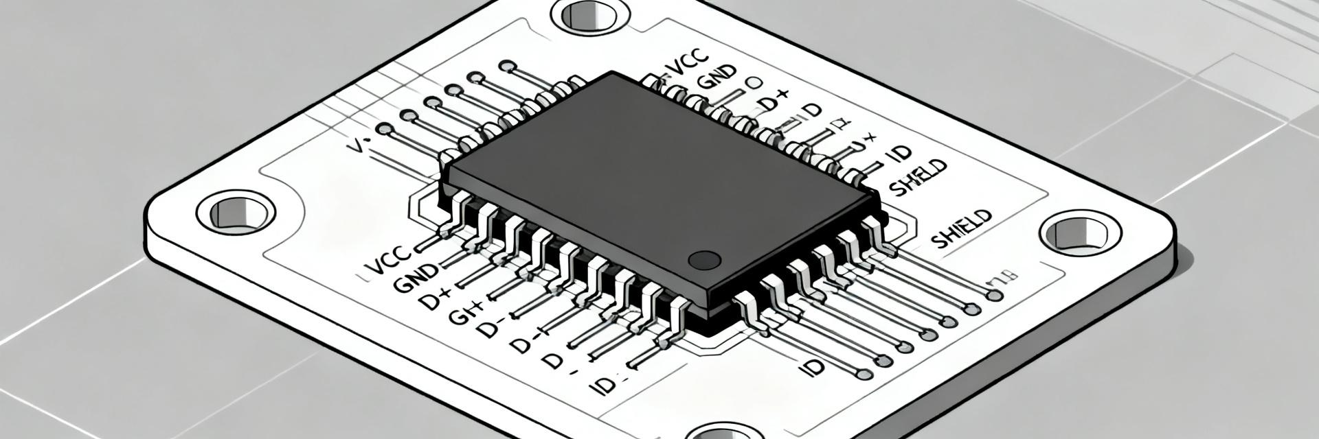
  • ISP1105BSTM: Pinout & Performance Summary — USB Transceiver

    USB 2.0 PHY HVQFN-16 12 Mbps FS 3.3V Logic The ISP1105BSTM is a compact low/full-speed USB transceiver supporting 1.5 Mbps and 12 Mbps operation with a typical supply window near 3.0–3.6 V and an HVQFN-16 footprint. This PHY-level component is designed for device-side integration in embedded systems, microcontroller peripherals, and battery-powered modules where full USB 2.0 high-speed (480 Mbps) is not required but reliability and power efficiency are paramount. 1 — ISP1105BSTM Overview & Primary Use Cases Point: The device serves as a PHY-level endpoint or device-side transceiver in embedded systems. Evidence: Datasheet excerpts list low/full-speed signaling and single-supply operation. Explanation: That combination makes it suitable for microcontroller peripherals, battery-powered accessories, and compact consumer modules. Constraints include a lack of 480 Mbps support and specific ESD limits that require external mitigation. 2 — Pinout & Functional Description The HVQFN-16 package arranges power, USB data, and ground pins around a central exposed pad. Critical pins require specific decoupling and pull-up resistor values for standard compliance. GND PAD VDD D- D+ VBUS_DET OE_N SUSP ISP1105BSTM HVQFN-16 Layout 2.1 Pin-by-pin recommendations Place 0.1 μF decoupling within 1–2 mm of VDD. Route D+/D- traces to external series resistors (22–33 Ω) for impedance tuning. The central exposed pad must be connected to the ground plane via thermal vias to ensure signal integrity and heat dissipation. 3 — Electrical Characteristics & Benchmarks Parameter Typical / Recommended Supply Voltage (VDD) 3.0 V – 3.6 V Data Rates 1.5 Mbps (LS) / 12 Mbps (FS) Quiescent Current 50–500 μA (mode dependent) Series Termination 22–33 Ω (External) Full-speed Pull-up 1.5 kΩ on D+ Differential Impedance 90 Ω ± 10% 4 — PCB Integration & Layout Checklist 4.1 Power and Grounding Implement a solid ground return path directly under the differential pairs. Use a 0.1 μF ceramic capacitor for high-frequency decoupling and a 1 μF bulk capacitor if VBUS sensing is used directly. Thermal vias on the HVQFN exposed pad are non-negotiable for stable ground references. 4.2 Signal Integrity Route USB signals as a coupled 90 Ω differential pair with matched lengths (within 10 mils). Avoid stubs and keep the distance between the transceiver and the USB connector as short as possible. Place common-mode chokes and TVS diodes at the board edge for EMI and ESD protection. 5 — Testing & Functional Verification A concise test plan includes verifying VDD/VBUS rails, checking USB line idle levels (J/K states), and monitoring successful enumeration with a host. Use an oscilloscope to measure rise/fall times against low/full-speed targets and evaluate common-mode excursions to identify termination issues early in the design cycle. FAQ What supply range does ISP1105BSTM require for reliable operation? Typical operation is within 3.0–3.6 V; design with margin below absolute max ratings and include local decoupling. Verify quiescent current and VBUS sensing behavior during initial power-up to ensure the system stays within thermal and power budgets. How should the pinout be protected from ESD when using this USB transceiver? Place bidirectional TVS or properly rated protection devices at the connector, keep series resistors close to the device, and implement ground stitching around the USB area. Verify protection components do not upset differential impedance or signal timing in compliance checks. Which PCB layout mistakes most commonly cause enumeration failures? Common errors include missing decoupling near VDD, incorrect pull-up values, long unmatched D+/D- traces, and poor ground return under the exposed pad. Use a methodical test checklist—power rails, idle line levels, and protocol traces—to isolate root causes quickly. What is the significance of the HVQFN-16 package's exposed pad? The central exposed pad of the HVQFN-16 package must be soldered to the PCB ground plane using multiple thermal vias. This provides the primary ground return path for high-speed signals and ensures efficient heat dissipation for the transceiver.
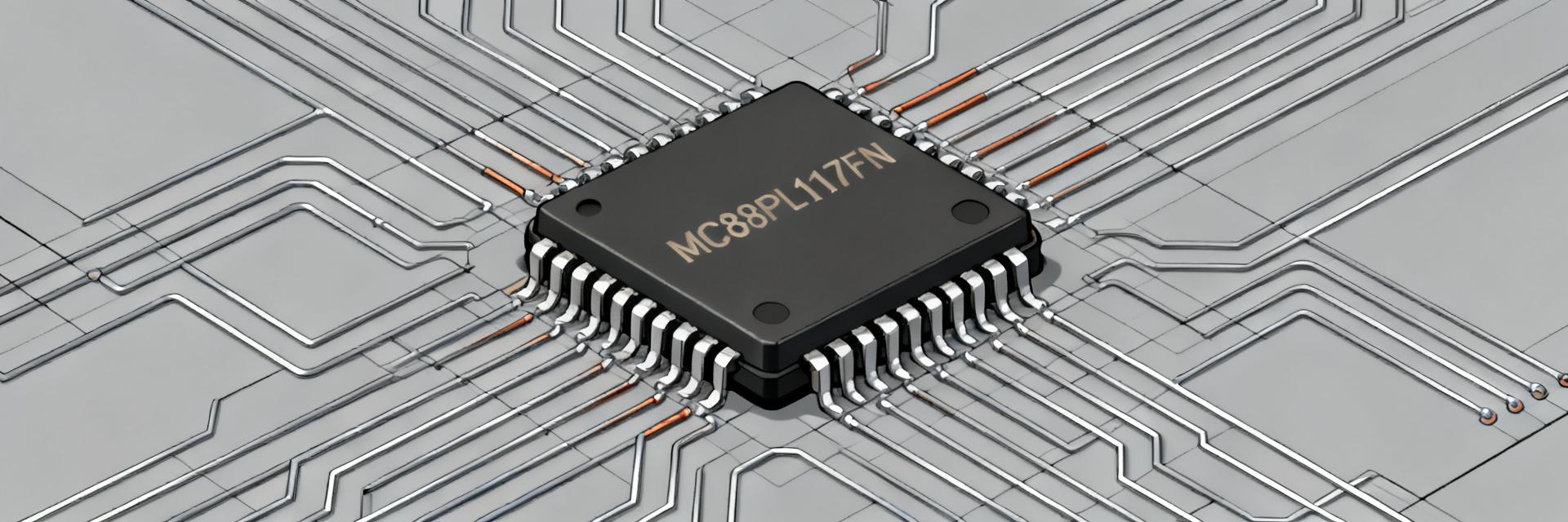
  • MC88PL117FN Datasheet Breakdown: Specs & Use Cases

    According to the MC88PL117FN datasheet, its PLL clock-driver architecture provides low-jitter frequency synthesis and multi-output clock distribution suitable for mixed-signal systems. A clear datasheet breakdown saves designers time, reduces revision cycles, and ensures correct thermal and timing margins during prototype and production phases. Product Overview & Key Takeaways The MC88PL117FN is a CMOS PLL clock driver intended to generate and distribute stable clock signals. Designers use it as a timing source feeding FPGAs, ADCs/DACs, and communication PHYs where low phase noise and multiple synchronized outputs reduce board-level jitter. MC88PL117FN PLL REF_IN Q0..Qn VCC GND (EPAD) ParameterValue (from datasheet)Test Conditions / Notes Supply Voltage Range3.0V to 3.6VNominal (3.3V) Max Supply Current (Icc)85 mA (Peak)All outputs switching @ 100MHz Output Drive / Load±24 mAVOH=2.4V, VOL=0.5V Lock Time< 10 msFrom cold-start to stable phase Thermal Limits (θJA)45 °C/WPLCC-28 Package on 4-layer PCB Deep Dive: Electrical Specifications Power Rails and Thermal Budgeting MC88PL117FN specs define absolute maximums and recommended operating ranges. Use the datasheet θJA to estimate junction temperature: Tj = Ta + (Pd × θJA). If operating at high ambient temperatures, ensure the exposed pad is stitched to a large ground plane to avoid thermal throttling. Implementation Checklist & Troubleshooting LAYOUT Place 0.1µF and 1µF decouplers within 2mm of each VCC pin. THERMAL Solder the exposed pad to a thermal land with at least 8 vias. SIGNAL Add 22Ω–33Ω series resistors on outputs for impedance matching. SymptomLikely CauseDebug Action OverheatingExceeded Pd per θJAMeasure Pd, check thermal via connectivity Unstable LockSupply noise / RippleVerify decoupling capacitors near VCC pins No OutputControl pin misstateCheck EN/SEL levels against logic thresholds Frequently Asked Questions What are the critical MC88PL117FN specs to validate in hardware? Focus validation on supply current (Iq/Icc), output drive capability under worst-case load, lock acquisition time, and thermal performance (θJA and Tj). Measure these under the datasheet test conditions and worst-case ambient/supply tolerances to ensure system margin. How should I size decoupling and thermal vias for the MC88PL117FN? Place a 0.1µF plus 1µF decoupling pair at each supply pin, within 1–2mm. Provide a soldered exposed pad with multiple thermal vias (typically 4–12 depending on board layer/copper) to reduce θJA; iterate with thermal calculations using Pd from the datasheet. Which bench tests most directly mirror datasheet curves for pass/fail? Run lock acquisition at nominal and extreme temperatures, load-step response to check output stability, and phase-noise/jitter measurements using the same load and supply conditions used in the datasheet plots. Define pass/fail thresholds from the datasheet tables. What is the primary function of the MC88PL117FN in digital systems? It serves as a low-jitter timing source to generate and distribute synchronized clock signals across digital and mixed-signal boards, feeding FPGAs and ADCs while minimizing phase noise across multiple domains.
  • 1201M2S3AV2KG2 Datasheet Deep Dive: Specs & Footprint

    The goal of this deep dive is to extract the measurable, design‑critical information engineers need from the component datasheet and convert it into a verified PCB footprint and validation plan. This introduction focuses on how to read the datasheet, prioritize sections, and capture the electrical and mechanical parameters that directly drive pad geometry, thermal strategy, and assembly constraints. 1 — Background & Typical Applications Device category & functional overview Point: Determine the component class and intended application spaces before committing to a footprint. Evidence: The datasheet title, ordering codes, and functional block diagram reveal the 1201M2S3AV2KG2 is a subminiature slide switch. Explanation: Identifying the device class informs expected tolerances and mounting robustness for applications like IoT modules and industrial controllers. Key datasheet sections to prioritize Point: Prioritize electrical characteristics, mechanical dimensions, and land patterns. Evidence: These sections contain pin count, pitch, and max height. Explanation: Extract pin numbering and nominal dimensions to create a checklist for CAD primitives, ensuring enclosure clearance and assembly compatibility. 2 — 1201M2S3AV2KG2 datasheet: Electrical & Mechanical Breakdown Electrical specifications to extract and verify Point: Extract absolute maximum ratings and operating ranges. Evidence: Datasheet tables for maximum conditions guide power budgeting. Explanation: Translate these into system constraints, defining decoupling and protection requirements. FieldValue (from datasheet)Design action Absolute Vmax[20V DC/AC]Clamp/protection, margin Operating V[0.4 VA max]Supply net assignment Max I or Pd[Record per Temp]Copper pour, thermal vias Timing / tR, tF[Contact Bounce]Signal integrity, debounce PIN 1 PIN 2 PIN 3 SWITCH BODY 3 — 1201M2S3AV2KG2 footprint: PCB Land Pattern & 3D Model IPC-compliant land pattern translation ItemTypical value Pad center-to-center[Verify Pitch: 2.54mm/5.08mm] Pad width / length[Lead size + Solder fillet] Paste aperture70–90% of pad area Mask openings0.05-0.1mm clearance 4 — Layout Integration & Manufacturing Thermal management and assembly Point: Determine thermal strategy based on θJA. Evidence: Datasheet thermal resistance indicates heat routing needs. Explanation: Place thermal via arrays under pads if power dissipation exceeds passive limits. Configure stencil apertures to prevent tombstoning during reflow. 5 — Validation Checklist FAI: Inspect solder fillet quality and placement accuracy against datum. Electrical: Continuity and insulation resistance per datasheet specs. Mechanical: Verify height clearance and actuator alignment for enclosure fit. Traceability: Document pad dimensions and pitch vs datasheet drawing. Frequently Asked Questions What are the critical datasheet items to verify before creating the footprint? Verify absolute maximum ratings, recommended operating conditions, pin-out and pin numbering, package outline with tolerances, recommended land pattern, and any assembly notes such as soldering temperature limits. How do I decide pad size and paste aperture from the datasheet? Base pad size on lead width and expected fillet, choosing a pad length that supports stable placement and fillet formation. Use paste aperture reductions (typically 70–90% of the pad) to control solder volume. Which tests validate that a footprint meets datasheet requirements? Run first article inspection checks (placement, fillet shape), electrical tests under nominal operating conditions, thermal measurement under worst-case power, and mechanical fit checks for height and mating interfaces. How is thermal management handled for 1201M2S3AV2KG2? If power dissipation exceeds board spreading capability, place a thermal via array under pads following a grid pattern (0.6–1.0 mm spacing) tied to internal copper pours; define measurement points near the hottest expected node. Summary Accurate interpretation of the 1201M2S3AV2KG2 datasheet ensures reliable assembly and long-term performance. By systematically extracting mechanical and electrical data, designers can create IPC-compliant footprints that minimize rework and optimize manufacturing yield.
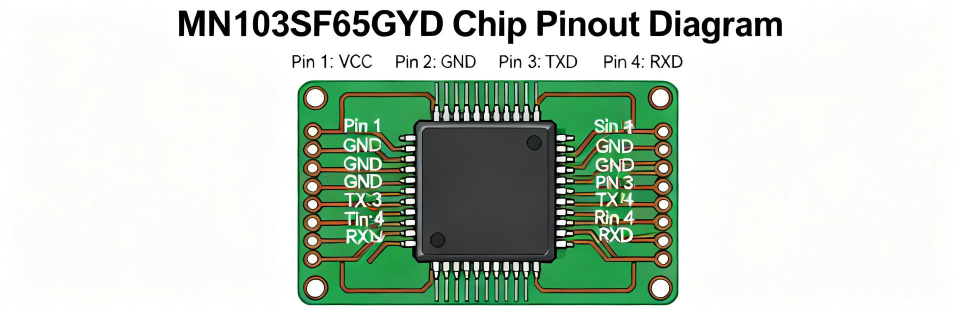
  • MN103SF65GYD Complete Datasheet & Pinout Overview Guide

    This guide condenses the MN103SF65GYD datasheet into a compact, engineer-focused reference for rapid design decisions. By focusing on measurable electrical limits and precise pin assignments, firmware and hardware teams can shorten prototype cycles and ensure long-term reliability. Background & Key Use Cases The MN103SF65GYD is a versatile embedded controller designed for low-to-mid-range sensor and power-management applications. Engineers select this IC for its compact footprint and integrated peripherals in cost-sensitive industrial designs. MN103SF65GYD (Top View) VCC GND TX RX ADC RST XTAL Pinout & Functional Grouping Pin # Pin Name Function Type 1VCCPrimary supply railPower 2GNDGround returnGround 3PA0 / UART_TXUART transmit / GPIOI/O 4PA1 / UART_RXUART receive / GPIOI/O 5ADC_IN0Analog input channel 0Analog 6RESETReset input (active low)Control 7XTAL_INExternal crystal inputClock 8NCNo connect / reserved— Core Implementation Guidelines Success with the MN103SF65GYD depends on respecting thermal and electrical boundaries. Key practices include placing 0.1µF decoupling caps within 2mm of VCC pins and isolating analog paths from digital return currents to maintain ADC precision. Common Questions What is the MN103SF65GYD pinout for UART/SPI? UART and SPI pins are multiplexed on programmable I/O banks. UART_TX/RX are usually on PA0/PA1. Map SPI to pins with the shortest trace lengths to external devices to minimize EMI. What supply voltages does MN103SF65GYD support? Consult the official datasheet for exact operating ranges. Design the power rail with headroom for transients and include voltage supervision to ensure clean startup. How to add decoupling caps for MN103SF65GYD? Use a 0.1µF ceramic capacitor close to each VCC pin, and a bulk 10µF capacitor near the regulator output to handle low-frequency transients and improve ADC stability. What are the recommended PCB layout tips? Maintain a star ground for analog pins, keep high-speed signals short, and use thermal vias under the package to dissipate heat effectively to the ground plane. Source: MN103SF65GYD Technical Documentation (Manufacturer Official Reference).