DMN5L06VK-7 MOSFET Performance: Data, Analysis & Specs
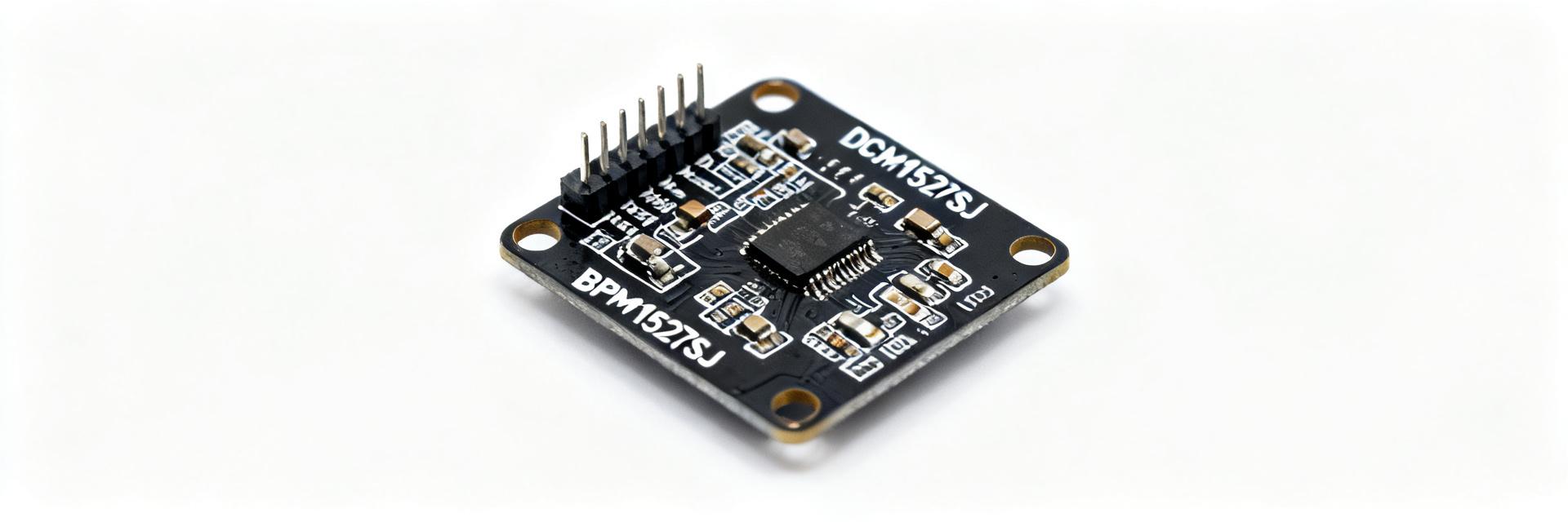
The DMN5L06VK-7 appears as a compact dual N‑channel switching device that combines a 50 V drain rating with a very low gate threshold (≈1.0 V max) and sub‑ohm class on‑resistance in a SOT‑563 footprint. These headline numbers matter: they enable battery‑powered and low‑voltage switching with minimal gate drive and small PCB area while keeping conduction losses low. This article breaks down the key specs, testing methods, benchmark expectations, layout guidelines and an actionable selection checklist.
1 — Product overview & key specs (background)

Electrical ratings & headline specs
| Parameter | Typical / Test | Interpretation |
|---|---|---|
| VDS | 50 V | Voltage margin for 12–36 V systems and transient safety headroom. |
| Continuous ID | ~280 mA | Suitable for low‑current load switching and signal loads. |
| VGS(MAX) | ±8–12 V | Limits gate drive amplitude; typical logic‑level drive recommended. |
| VGS(th) (max) | 1.0 V | Allows reliable switching with low logic voltages (1.8V/2.5V/3.3V). |
| RDS(on) | Sub-ohm range | Primary determinant of conduction loss; consult test‑condition tables. |
| Package | SOT‑563 | Ultra-small dual channel footprint for space‑constrained designs. |
Package, pinout & thermal constraints
SOT‑563 is a 6‑lead micro package with two MOSFET channels; pin assignments place drains and sources across the tiny footprint so board copper is critical. Junction‑to‑ambient thermal resistance is high compared with larger packages. Recommended practice: maximize copper pour on the drain plane, add at least 4–8 thermal vias (0.3–0.4 mm) to an internal ground plane.
2 — Datasheet deep-dive (data analysis)
Interpreting RDS(on) and Temperature Coefficients
Point: RDS(on) rises with falling VGS and with increasing Tj. Evidence: datasheet RDS(on) is specified at defined VGS/test temp. Explanation: to estimate in‑system loss, convert the datasheet RDS(on) at test conditions to operating Tj using the temperature coefficient curve. For ID=0.3 A and RDS(on)=0.6 Ω, P = I²·R = 0.09 W.
Capacitances and Switching Behavior
| Drive Voltage | Assumed Qg | Relative switching energy |
|---|---|---|
| 4.5 V | 8 nC | ~36 nJ (Lower gate energy) |
| 10 V | 8 nC | ~80 nJ (Higher EMI risk) |
3 — Benchmarks & Test Methods
Point: Repeatability requires tight control of VGS, VDS, and temperature. Evidence: best practice uses Kelvin sensing for RDS(on). Explanation: 1) Mount sample on representative PCB; 2) Measure static RDS(on) via 4‑wire sense; 3) Capture gate/drain waveforms; 4) Report Tj behavior. Watch for lead resistance biasing and self-heating effects.
4 — Design Integration & Layout
- Low‑side battery load switch: Microcontroller GPIO driven, <0.1 W conduction at 300 mA.
- Dual‑channel management: Two channels control separate subsystems to save BOM.
- PCB Layout: Short, wide traces on drain/source, minimal loop area for gate drive, 4-8 thermal vias under drain.
5 — Comparative Case Studies & Checklist
Scenario A: Handheld battery sensor <300 mA—choose for 50V margin and low VGS(th). Scenario B: Peripheral power switching—dual channels simplify BOM and match characteristics.
Procurement & Troubleshooting FAQ
What are the primary applications for the DMN5L06VK-7?
It is optimized for low-side battery load switching, dual-channel load management, and auxiliary paths in small DC-DC converters where space and logic-level drive are critical.
How should the SOT-563 package be thermally managed?
Maximize copper pour on the drain plane and use 4–8 thermal vias (0.3–0.4 mm) to connect to internal ground planes to mitigate the high junction-to-ambient thermal resistance.
What is the typical gate threshold voltage for this MOSFET?
The VGS(th) is typically around 1.0V (max), which allows it to be driven reliably by low-voltage logic levels directly from microcontrollers.
Why is RDS(on) variation important in the design phase?
RDS(on) increases with junction temperature and lower VGS. Designers must use datasheet curves to estimate real-world conduction losses at operating temperatures to avoid thermal throttling.
Summary
The DMN5L06VK-7 delivers a compact dual N‑channel solution with a 50 V rating and low gate threshold. Key takeaway: maximize drain copper and validate RDS(on) at operating temperatures for reliable high-density designs.