BSC190N12NS3G MOSFET: Complete Spec Report & Bench Data
Point: This consolidated spec-and-bench report frames why a focused datasheet review plus measured bench data matter for design tradeoffs. Evidence: Designers must compare rated VDS, RDS(on), gate charge, and thermal limits against real-world measurements. Explanation: A concise view lets engineers decide if the device suits 120 V-class switching regulators, synchronous buck stages, or motor-drive half-bridges.
Point: The report covers three focal data types: datasheet static/thermal specs, independent bench data, and practical design implications. Evidence: Each section links test conditions to measured results to support selection or derating. Explanation: That approach reduces late-stage surprises by verifying RDS(on), V(BR), gate charge, switching losses, and thermal rise under representative conditions.
1 — Background & Key Spec Snapshot
1.1 — Quick Spec Table
| Parameter | Typical Value | Test Condition |
|---|---|---|
| VDS (rated) | 120 V | — |
| Continuous ID | ~100 A | Per datasheet pulse/DC notes |
| RDS(on) | ~0.020–0.050 Ω | VGS = 10 V / 4.5 V |
| Total Gate Charge Qg | ~30–60 nC | VGS sweep 0→10 V |
| Max Pd | Package Dependent | TJ = specified limit |
| Junction Temp | -55 to +175 °C | Industrial Rating |
2 — Datasheet Deep-Dive: Static & Thermal
Prioritize breakdown V(BR)DSS, ID limits, and RDS(on) at various VGS points. Low Vth and low RDS(on) at target VGS reduce conduction loss; high leakage or borderline V(BR) requires voltage margin for 120 V systems. Use RθJA and RθJC plus package thermal path to estimate junction rise. ΔTj ≈ Pd × RθJA for free-air; provide copper area and heatsink to lower effective RθJA.
3 — Bench Test Methodology & Setup
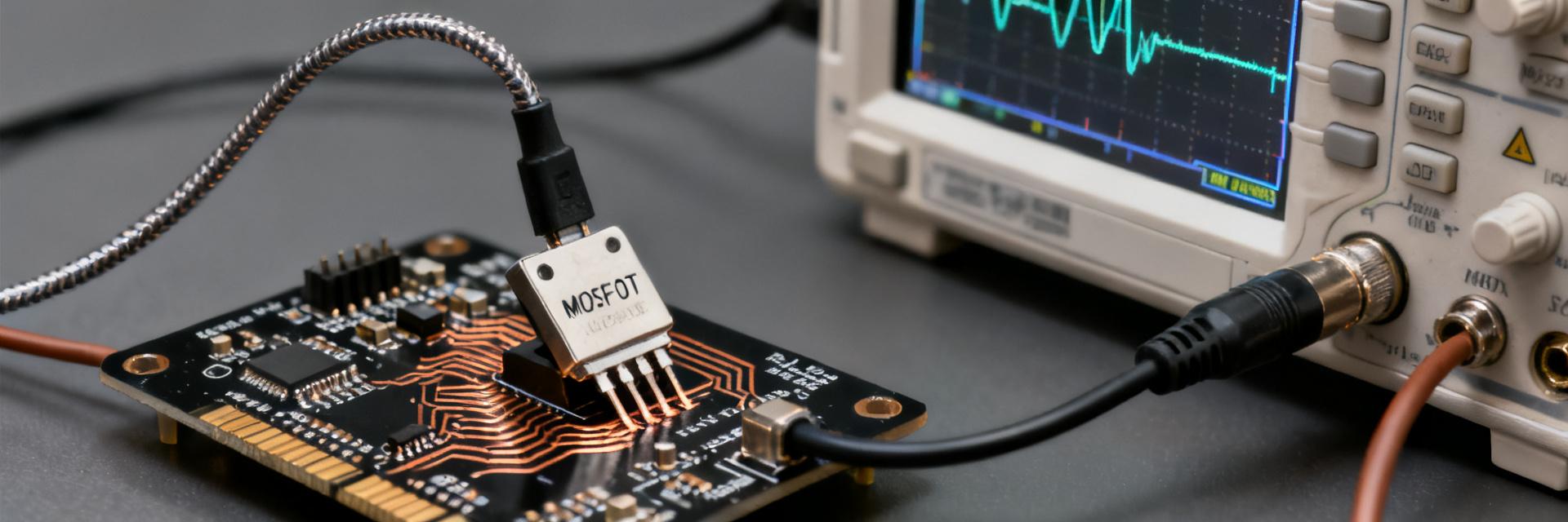
Reproducible bench data requires a low-inductance fixture and Kelvin sense. Recommended gear includes pulse-capable power supplies and high-bandwidth probes. Follow pulse methods (≤1 ms) to measure RDS(on) to avoid self-heating. Log data in CSV with timestamps and ambient temp to enable comparison to datasheet figures.
4 — Bench Results & Analysis
Present RDS(on) vs VGS and temperature. Expect measured RDS(on) to differ slightly from datasheet due to sample variance. If measured RDS(on) is higher at room temp, that gap often widens with temperature. For safety, derate continuous current or increase cooling to recover margin.
5 — Practical Design Checklist
- Maintain VDS margin >20% relative to 120V rating.
- Derate ID per thermal model and copper pour area.
- Choose VGS drive (10V preferred for lowest RDS(on)).
- Set gate resistor and layout for low inductance.
- Match RDS(on), Qg, and RθJA when substituting parts.
Summary
BSC190N12NS3G offers a balanced tradeoff for many 120 V applications but requires attention to gate drive and cooling. Run RDS(on), gate charge, and switching energy tests before committing to high-volume production.
Frequently Asked Questions
What bench tests confirm RDS(on) suitability?
Measure RDS(on) using short pulses (≤1 ms) at your target VGS points and log ambient and junction estimates. Use Kelvin sensing, report uncertainty, and repeat at elevated temperature to understand operating behavior under real load.
How should I model thermal limits for continuous operation?
Use Pd × RθJA to estimate junction rise for free-air conditions and prefer RθJC with a defined heatsink for conservative estimates. Include copper pour recommendations, and validate with a thermal ramp test.
Which three tests are highest priority before production?
The minimal verification set: (1) pulse RDS(on) at operating VGS and temperature, (2) gate charge and switching-energy measurement, and (3) thermal ramp/steady-state power test with intended PCB mounting.
What gate drive voltage is recommended for the BSC190N12NS3G?
A VGS of 10V is recommended to achieve the rated RDS(on) and minimize conduction losses, as specified in the datasheet static characteristics.