RGP10M-E3 Diode: Full Specs & Performance Breakdown
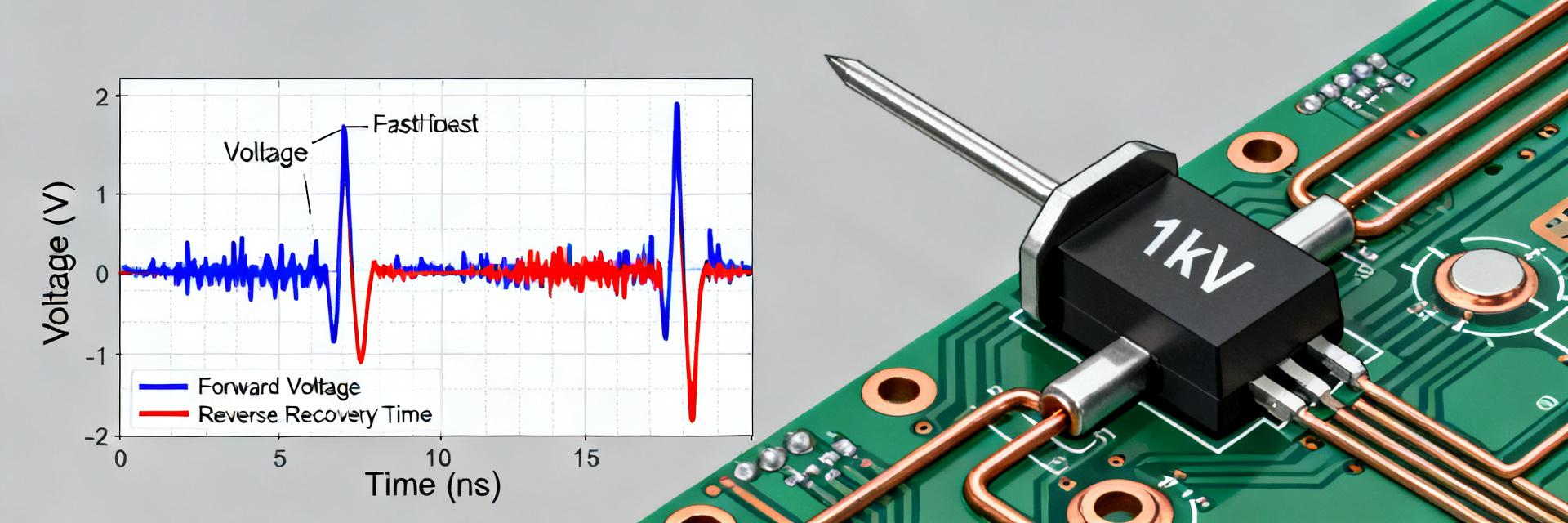
The RGP10M-E3 diode is engineered for high-reliability rectification, featuring a repetitive peak reverse voltage of 1000 V and an average forward current of 1 A. With a typical forward voltage (Vf) of ~1.3 V and a reverse-recovery time (trr) of approximately 500 ns, this device serves as a robust 1 kV-class fast recovery rectifier. For power-switching applications, these specifications provide a significant voltage margin for high-voltage rails while maintaining manageable conduction losses at 1 A, though switching losses and EMI must be monitored at higher kHz-range frequencies.
1 — Background & Typical Applications
1.1 — What the part is and where it fits
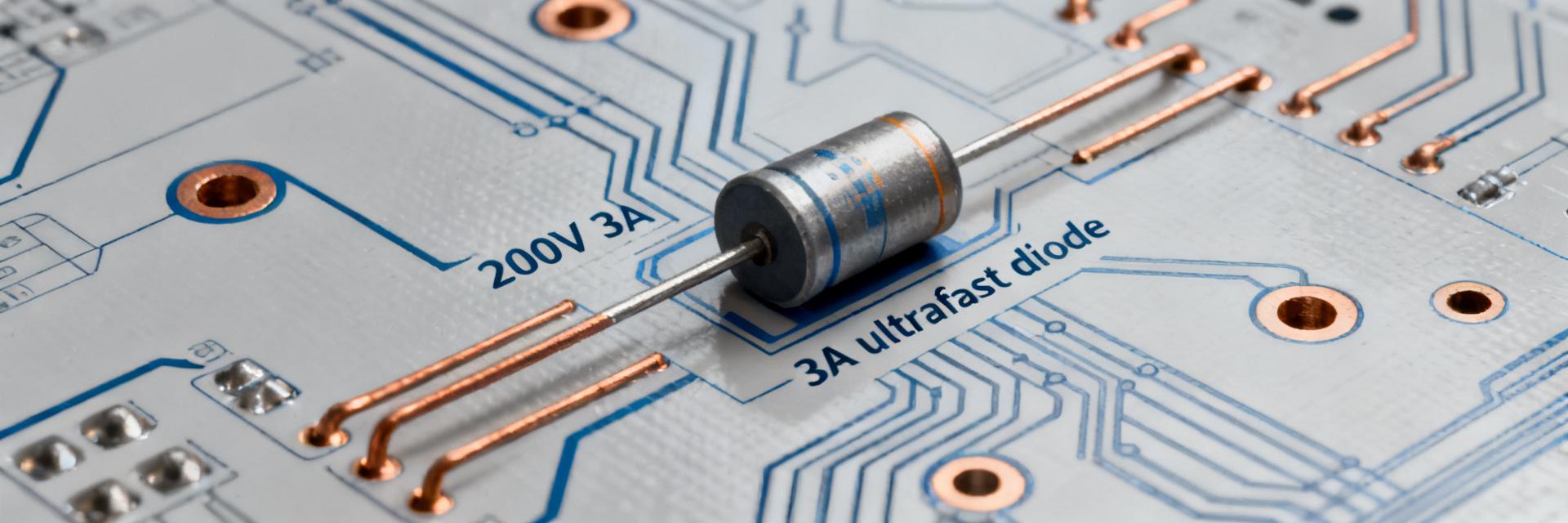
The RGP10M-E3 is a glass-passivated fast recovery switching rectifier housed in a through-hole DO-204AL (DO-41) axial package. Its architectural design prioritizes high-voltage durability, making it a staple in power supplies, inverters, and freewheeling/recirculation circuits where peak inverse voltage (PIV) rating is more critical than ultra-low conduction loss.
1.2 — Key electrical context to know up front
Designers must evaluate VRRM, IF(AV), IFSM, trr, and thermal resistance as primary filters. High-voltage switching demands VRRM margin and surge capability, while high-frequency operations require careful analysis of trr and di/dt behavior to minimize switching energy dissipation.
2 — Performance Specs Deep-Dive
2.1 — Voltage, current, and thermal limits
Quantitative limits are defined by 1000 V VRRM and 30 A single-pulse surge capability. For long-term reliability, engineers should target 60–75% of the rated VRRM for inductive switching margin and derate IF(AV) based on the junction-to-ambient thermal path.
| Parameter | Typical / Datasheet Condition |
|---|---|
| Repetitive Reverse Voltage (VRRM) | 1000 V |
| Average Forward Current (IF(AV)) | 1.0 A |
| Surge Current (IFSM) | 30 A (8.3 ms half-sine) |
| Typical Forward Voltage (Vf) | 1.3 V @ 1 A |
| Reverse Recovery Time (trr) | 500 ns |
2.2 — Switching behavior: recovery time and losses
Conduction losses are estimated as Pcond ≈ Vf × Iavg. At higher frequencies, switching energy (Esw ≈ 0.5 × Vpeak × Ipeak × trr) becomes dominant. With a 500 ns recovery time, the RGP10M-E3 is efficient in the low-to-mid kHz range, but requires careful snubber design if pushed into high-frequency domains.
3 — Comparative Benchmarks
| Category | Strength | Trade-off |
|---|---|---|
| Fast Recovery (RGP10M) | High VRRM (1kV), Robust | Moderate trr (500ns) |
| Ultra-Fast Type | Low trr (<100ns) | Higher cost, lower VRRM |
| Schottky Diode | Zero trr, Low Vf | Low VRRM (<200V) |
4 — Design & Testing Best Practices
Minimize loop inductance by keeping lead lengths short and utilizing copper pours for axial pad heat spreading. During validation, capture peak recovery current and junction rise (ΔTj) using clamped inductive load setups to ensure the device operates within its safe operating area (SOA).
Summary
- When to use: Ideal for high-voltage switching where 1 kV margin and robustness are prioritized over ultra-fast recovery.
- Key tests: IV sweep, trr capture, and thermal logging under expected duty cycles.
- Derating: Operate at ≤75% VRRM; treat surge rating as single-pulse only.
Frequently Asked Questions
Is the RGP10M-E3 diode suitable for high-frequency switching?
It can be used at moderate frequencies. With trr ≈500 ns, switching energy grows with frequency, increasing EMI and loss. For frequencies above a few hundred kHz, consider ultra-fast types or Schottky alternatives.
What are the critical specs to check on the official datasheet?
Prioritize VRRM (1000V), IF(AV) (1A), IFSM (30A), Vf (1.3V), and trr (500ns). Ensure test conditions (TC, pulse width) match your specific application requirements.
How should engineers estimate losses for thermal design?
Calculate conduction loss (Pcond ≈ Vf × Iavg) and switching energy per transition. Combine these for total dissipation and compare against θJA/θJC to keep junction temperature within safe limits.
What are the recommended mounting practices for RGP10M-E3?
Minimize lead lengths to reduce parasitic inductance, use copper pours for heat spreading, and ensure proper solder fillets to optimize the thermal path to the PCB.