L07P003D15 datasheet: Full electrical specs & test data
The L07P003D15 presents headline figures that guide design expectations: 3 A continuous current rating, ~5 µs step response, ±15 V recommended supply rails, ≈30 mA supply current, operating range −30 °C to 80 °C, usable bandwidth near 100 kHz, and bidirectional sensing capability. This article functions as a compact L07P003D15 datasheet-style reference focused on electrical specs, reproducible test data, measurement methods and pragmatic guidance for designers and test engineers.
Background & product overview

What the L07P003D15 is and typical use cases
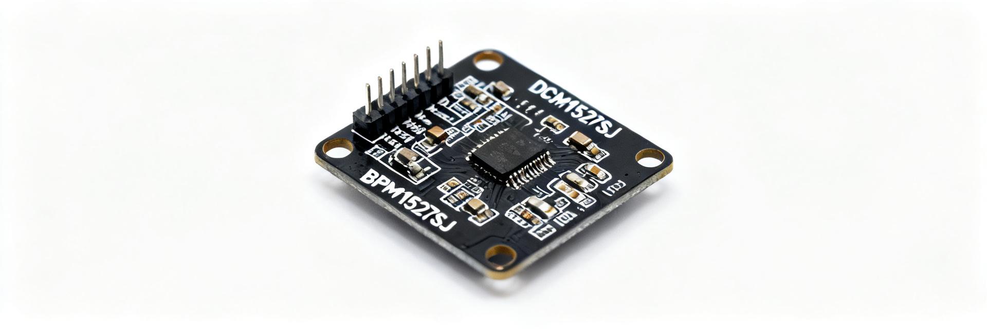
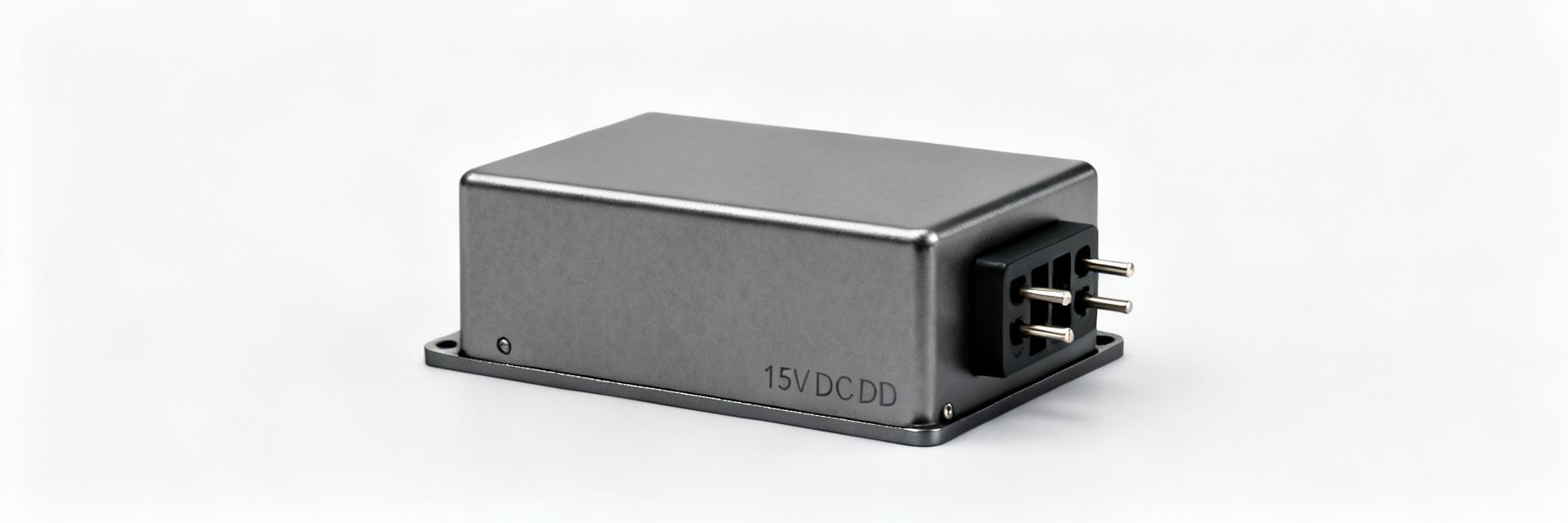
The L07P003D15 is an open-loop PCB-mounted current sensor providing voltage-output proportional to conductor current for bidirectional measurement. It targets low-to-medium current monitoring with a compact pass-through conductor optimized for PCB assembly. Typical domains include power monitoring, motor control current feedback, battery management system sensing, and instrumentation.
Package, pinout and key mechanical info
- Pins: VCC (+15V), GND (0V), VOUT (Analog Out), I+ / I− (Sensing Path)
- Mounting: PCB through-hole; maintain recommended creepage/clearance.
- Footprint note: Keep adjacent copper clear for the sense path to avoid magnetic interference.
Full electrical specifications
| Parameter | Typical | Min/Max | Conditions |
|---|---|---|---|
| Supply Voltage | ±15 V | ±12 V / ±15 V | Dual rails, decoupled |
| Input Current | 3 A | 3 A Max | Continuous, ambient cooling |
| Supply Current | 30 mA | 40 mA Max | Per rail total |
| Response Time | 5 µs | — | 10-90% of step |
| Bandwidth | 100 kHz | — | -3 dB point |
| Op Temp | — | -30 to 80 °C | Ambient environment |
Typical performance and validation test data
Reproducible measurement requires defined fixturing. A recommended test bench includes a low-noise power supply, precision current source, and an oscilloscope with ≥1 MHz BW. Use supply decoupling at the device (0.1 µF + 10 µF) and twisted routing for the sense conductor to minimize noise pickup.
Test checklist & troubleshooting guide
| Symptom | Probable cause | Corrective action |
|---|---|---|
| Large offset at 0 A | Residual magnetization | De-magnetize fixture; re-zero |
| High noise | External EMI | Improve grounding; add shielding |
| Saturation | Exceeded linear limit | Reduce input current; check VCC |
| Slow response | Excessive RC filtering | Adjust filter cutoff frequency |
Summary & Key Takeaways
- Device Role: PCB-mounted open-loop sensor for 3A power monitoring.
- Electrical Focus: Linear output with 100kHz bandwidth and 5µs response.
- Validation: Use two-point calibration (Zero and Full Scale) for optimal ADC mapping.
FAQ
How do I interpret the L07P003D15 zero offset and calibrate it?
Measure VOUT with 0 A in the conductor after thermal soak. Record the zero offset, apply a precision known current and measure gain. Use two-point calibration to derive offset and gain correction.
What test data should I collect to verify bandwidth and response time?
Collect step-response waveforms (10–90% rise/fall) using a fast current step and an oscilloscope with bandwidth >1 MHz. Capture frequency sweep amplitude up to the –3 dB point.
What are common sources of measurement error and how are they mitigated?
Primary sources are external magnetic fields and EMI. Mitigate by keeping sense paths short, using decoupling capacitors within 3mm of pins, and implementing local shielding.
What is the recommended supply voltage and temperature range?
The device operates optimally with a ±15V supply (range ±12V to ±15V) within an ambient temperature range of -30°C to 80°C.