-
- Contact Us
FDP027N08B MOSFET Datasheet Deep-Dive: Key Specs & Test Data
The FDP027N08B is a high‑current N‑channel PowerTrench MOSFET rated at 80 V with sub‑3 mΩ on‑resistance and continuous currents specified above 200 A—parameters that make it a go‑to for motor drives, DC‑DC converters and power supplies. This deep‑dive decodes the FDP027N08B datasheet and typical test data so engineers can quickly assess fit, limits and test methods for real designs. (Source: onsemi datasheet)
Point: summarize intent and immediate applicability. Evidence: the manufacturer’s datasheet lists the device’s key limits and test conditions that form the basis for safe use. Explanation: designers should map datasheet conditions to system conditions (gate drive, temperature, PCB thermal path) before committing to the device. Link: manufacturer datasheet is the primary reference (onsemi datasheet).
1 — Background & Product Overview (type: background)

What the FDP027N08B is and where it came from
Point: device identity and lineage. Evidence: the FDP027N08B is listed in onsemi’s low/medium voltage MOSFET portfolio and appears in historical Fairchild/ON heritage catalogs. Explanation: it is a silicon PowerTrench N‑channel optimized for low RDS(on) in a through‑hole TO‑220‑3 style package, intended for high‑current low‑voltage switching such as motor drive low‑side, synchronous rectification and power distribution. The part is commonly cross‑referenced on distributor pages where stock may be intermittent; lifecycle status can vary by supplier, so sourcing should check manufacturer stock and lifecycle notes. Link: consult the manufacturer datasheet and distributor pages for sourcing and lifecycle confirmation (onsemi datasheet).
Core electrical ratings at a glance
Point: headline ratings designers check first. Evidence: datasheet typical entries include VDS = 80 V, continuous drain current listed (e.g., ~223 A depending on mounting and Tc), maximum VGS ±12 V or ±20 V on some sheets, maximum junction temperature Tj,max = 175°C, and RDS(on) typical vs max reported at specified VGS and 25°C. Explanation: the 80 V rating and very low RDS(on) make the device suited for sub‑80 V systems, but continuous current figures assume ideal thermal sinking—real continuous current must be derated for PCB thermal resistance and ambient. Rule of thumb: limit VGS drive to the datasheet recommended safe gate drive (commonly 10–12 V), derate RDS(on) for temperature (roughly a linear increase with junction temperature per the RDS(on) vs Tj curve). Link: key ratings are summarized from the official datasheet (onsemi datasheet).
Typical package, thermal and mechanical notes
Point: package and thermal behavior. Evidence: the package listed is a TO‑220‑3 style PowerTrench package with defined RθJC and RθJA in the datasheet; typical RθJC is low (single‑digit °C/W) while RθJA depends heavily on board copper and mounting. Explanation: for bench and production, use a dedicated heatsink or large copper area, proper mounting torque and an insulating pad if required. For screw mounting, follow torque specs in the mechanical notes and use a mica or silicone insulator when isolation is needed; ensure thermal grease or pad is applied to reduce interface thermal resistance. Link: mechanical drawings and thermal resistance numbers are documented in the datasheet (onsemi datasheet).
| Parameter | Value (typ) | Notes / Test Conditions |
|---|---|---|
| VDS | 80 V | Drain‑Source breakdown rating |
| Continuous ID | ~223 A | Case‑based rating, requires heatsink |
| RDS(on) | sub‑3 mΩ (typ) | Measured at VGS = 10 V, Tj = 25°C |
| VGS,max | ±12 V (typ) | Check sheet variant for ±20 V listings |
| Tj,max | 175 °C | Maximum junction temperature |
| Package | TO‑220‑3 / PowerTrench | Through‑hole, screw mount |
2 — Datasheet Key Specifications Explained (type: data analysis)
RDS(on): measurement conditions and real-world meaning
Point: RDS(on) is the primary determinant of conduction loss. Evidence: the datasheet gives RDS(on) at specific VGS (commonly 10 V) and at 25°C, with typical and maximum columns; an RDS(on) vs temperature curve shows increase with Tj. Explanation: to estimate conduction loss use P = I^2 × RDS(on). Example: at 100 A and RDS(on) = 3 mΩ, P = 100^2 × 0.003 = 30 W dissipated in the MOSFET—this is junction heating requiring substantial thermal path. Designers should calculate junction rise using ΔTj = P × RθJC (for short pulses) or P × RθJA (steady state on PCB). Link: values and temperature curves are available in the datasheet (onsemi datasheet).
Avalanche, SOA and switching limits
Point: avalanche energy and SOA limit inductive switching. Evidence: the datasheet provides single‑pulse avalanche energy and often SOA charts showing allowable VDS/ID combinations for given pulse widths. Explanation: single‑pulse avalanche is not a license for repetitive transients—designers should derate for repetitive or high‑frequency transients and use snubbers or TVS diodes for inductive loads. When switching inductive loads, ensure the energy per event and repetition rate keep junction excursions within limits; use SOA curves to confirm safe operating envelopes. Link: avalanche and SOA data are specified in the datasheet (onsemi datasheet).
Gate characteristics and switching performance
Point: gate charge and capacitances determine switching behavior. Evidence: datasheet lists VGS(th), total gate charge QG at specified VGS and VDS, and parasitic capacitances Ciss, Coss, Crss. Explanation: QG sets the energy the gate driver must supply; switching loss approximation due to gate charging is Egate ≈ QG × Vdrive, and switching losses on the drain are influenced by dv/dt and Miller capacitance (Crss). For example, a gate drive of 10 V and QG = 60 nC implies ~0.6 mJ per switching transition, which at 100 kHz equals 60 W in gate drive energy (split between turn‑on and turn‑off efforts and driver dissipation). Choose a gate driver with adequate peak current and control turn‑on dv/dt via series gate resistors to manage overshoot. Link: gate charge and capacitance tables are in the datasheet (onsemi datasheet).
3 — Typical Test Data & Performance Analysis (type: data analysis)
Interpreting the datasheet’s typical curves
Point: which curves to inspect and how. Evidence: typical datasheet curves include ID vs VDS, transfer characteristics (ID vs VGS), RDS(on) vs Tj, and switching waveforms. Explanation: read ID vs VDS to understand linear/ohmic regions and saturation onset; use transfer curves to determine required VGS for a target ID; use RDS(on) vs Tj to derate conduction loss at elevated temperature. Extract design points by reading the current at the gate voltage you can supply and then applying thermal derating. Link: these typical curves are included in the manufacturer’s datasheet (onsemi datasheet).
Example performance calculations from test data
Point: worked examples speed decision making. Evidence: using datasheet RDS(on) and thermal numbers supports concrete estimates. Explanation: example 1 — conduction loss at 150 A with RDS(on) = 3 mΩ: P = 150^2 × 0.003 = 67.5 W. Example 2 — junction rise for steady 67.5 W on a board with RθJA = 1.0 °C/W (heatsink case will be lower): ΔTj ≈ 67.5 × 1.0 ≈ 67.5 °C above ambient; ensure Tj,max not exceeded. Example 3 — switching loss estimate at 50 kHz with VDS transition of 48 V and ID = 50 A over 50 ns: energy per transition E ≈ 0.5 × V × I × t ≈ 0.5 × 48 × 50 × 50e‑9 ≈ 60 µJ, switching power Psw = E × f ≈ 3 W. Sum switching and conduction losses for total device dissipation and compare against thermal budget. Link: use datasheet curves and numbers for input parameters (onsemi datasheet).
Comparing datasheet vs measured results (what diverges)
Point: expect lab vs sheet differences. Evidence: datasheet conditions are tightly controlled (pulse widths, fixture thermal anchoring, Kelvin senses). Explanation: real bench or production measurements often show higher RDS(on) and switching losses due to contact resistance, long leads, PCB thermal limitations, and thermometer placement. Mitigate by using Kelvin sense for RDS(on), controlled pulse widths to avoid self‑heating, and replicate the datasheet test fixture as closely as possible. Link: measurement pitfalls and recommended corrections are summarized from measurement best practices and datasheet test notes (onsemi datasheet).
4 — How to Test FDP027N08B: Measurement Methods & Test Setup (type: method guide)
Recommended bench setup for RDS(on) and transfer curve tests
Point: recommended measurement hardware and procedure. Evidence: standard practice uses a precision source meter or pulsed current source, pulse generator for gate, oscilloscope and Kelvin sense wiring; datasheet lists pulse conditions to avoid self‑heating. Explanation: mount the device on a metal plate or heatsink, use Kelvin connections for drain/source, choose pulse widths (e.g.,
Switching tests: layout and measurement tips
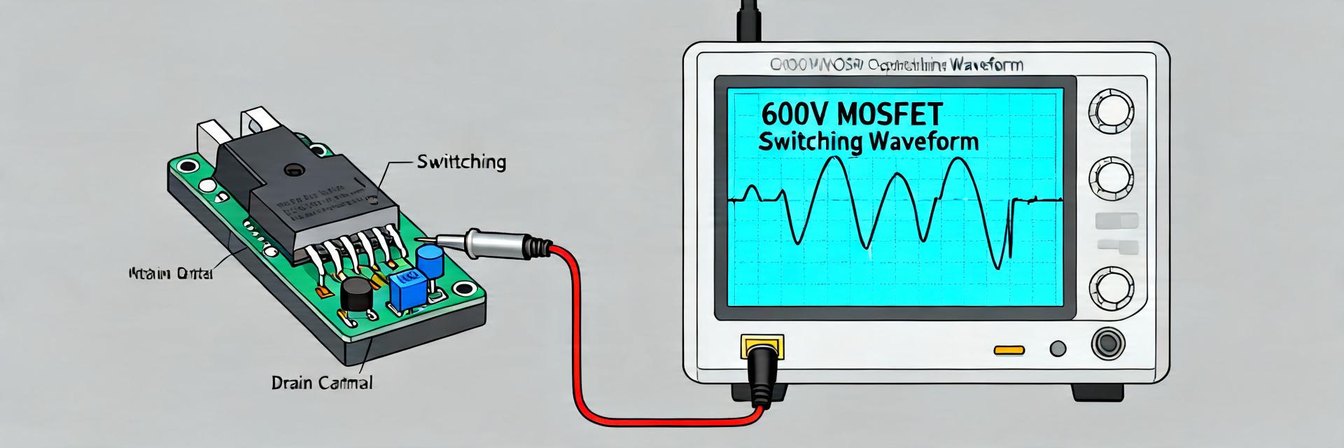
Point: layout and probe placement matter most in switching tests. Evidence: parasitic inductance in loop leads to overshoot and ringing; datasheet switching waveforms assume low‑parasitic fixtures. Explanation: minimize loop area for the drain‑source current path and place the current probe around the DC return or use a Rogowski/probe close to the device. Use a high‑bandwidth differential probe for VDS and a low‑inductance current probe. Add small series gate resistors to tune dv/dt and reduce ringing; capture both voltage and current waveforms at the same time to compute switching energy. Link: measurement layout guidance is consistent with datasheet test descriptions (onsemi datasheet).
Thermal characterization and junction temperature estimation
Point: practical methods to find RθJC and RθJA. Evidence: datasheet provides RθJC and example RθJA for reference PCB; for accurate validation use thermocouples and IR imaging. Explanation: attach a fast thermocouple to the package tab for approximate case temperature and use IR imaging to map hot spots on the die area (account for emissivity). For RθJC, short power pulses and measure junction‑to‑case rise; for RθJA use steady‑state power and measure ambient‑to‑case difference. Use these to calibrate thermal model and estimate junction temperature under expected duty cycles. Link: thermal measurement methods align with the datasheet’s thermal notes (onsemi datasheet).
5 — Practical Recommendations: Selection, Substitutes & Design Considerations (type: action/case)
When to choose the FDP027N08B (and when not to)
Point: application fit guidance. Evidence: given low RDS(on), high ID rating and 80 V rating, the device is ideal for high‑current low‑voltage switching such as motor low‑side switches, DC bus distribution and synchronous rectifiers. Explanation: avoid the part for extremely high‑frequency switching (>200–300 kHz) where package inductance and gate charge impair efficiency, or where SMD form factor is mandatory. If the design requires repetitive avalanche tolerance or extreme SOA margins, choose a device with explicit repetitive avalanche or higher SOA margins. Link: application guidance derived from datasheet electrical and SOA data (onsemi datasheet).
Common substitutes and cross-reference guidance
Point: substitution strategy. Evidence: replacement should match VDS, RDS(on) at VGS, package thermal specs and total gate charge QG. Explanation: when cross‑referencing, ensure pinout and mounting form factor match (TO‑220‑3 screws and tab footprint differ across makers), and verify SOA and avalanche specs; test suspected substitutes under realistic thermal and switching conditions before committing. Link: use datasheet comparisons and vendor cross‑reference tables for candidates (manufacturer datasheets).
PCB layout, gate drive and thermal best practices
Point: concrete layout and drive tips. Evidence: datasheet switching examples and general best practices show the impact of loop inductance and gate drive impedance. Explanation: keep the switching loop (Vbus, device, return) as small as possible; use a short Kelvin source trace to the current sense resistor if present; place the gate driver close to the MOSFET, use a small series gate resistor (tune for rise/fall balance), and include snubbers or RC damping for inductive loads. For thermal, allocate generous copper area, thermal vias under the device pad, and a heatsink or forced airflow to meet RθJA targets and maintain junction below Tj,max. Link: layout and thermal recommendations are consistent with datasheet test notes and industry best practices (onsemi datasheet).
Summary
- The FDP027N08B is an 80 V, very low RDS(on) power MOSFET suited to high‑current low‑voltage switching; verify gate drive and thermal path against datasheet test conditions before use (FDP027N08B reference: onsemi datasheet).
- Use pulsed RDS(on) tests with Kelvin sensing and replicate datasheet pulse widths to avoid self‑heating; calculate conduction loss with P = I²R and combine with switching loss estimates from QG and measured dv/dt.
- For switching tests, minimize loop inductance, use appropriate gate resistors and capture VDS/ID with high‑bandwidth probes; thermally, design for worst‑case ambient and required heatsinking using RθJA/RθJC guidance.
6 — FAQ
What is the recommended gate drive voltage for this MOSFET?
Answer: The datasheet lists test conditions at VGS = 10 V for typical RDS(on) performance, and maximum allowable gate voltage is shown as ±12 V on common documentation. Use a stiff 10–12 V gate drive for lowest RDS(on), avoid over‑voltage on the gate and ensure the driver can source the peak current required by the device’s QG. (Source: onsemi datasheet)
How do I estimate junction temperature for a given steady current?
Answer: Calculate conduction and switching losses using datasheet RDS(on) and switching energy estimates, sum to get total device power P. Multiply P by RθJA (board‑dependent) to get ΔT above ambient, then add ambient to get estimated Tj. For short pulses use RθJC for transient junction rise. Verify with thermocouples or IR imaging against datasheet thermal limits. (Source: onsemi datasheet)
Are there direct drop‑in SMD equivalents for this through‑hole part?
Answer: Direct drop‑in SMD equivalents are uncommon because thermal and parasitic behaviors differ; when substituting to an SMD device, match VDS, RDS(on) @ VGS, Qg and package thermal performance, and validate pinout and SOA. Always bench‑test the substitute in your application conditions. (Source: manufacturer and distributor datasheet comparisons)
- Technical Features of PMIC DC-DC Switching Regulator TPS54202DDCR
- STM32F030K6T6: A High-Performance Core Component for Embedded Systems
- Tamura L34S1T2D15 Datasheet Breakdown: Key Specs & Limits
- PAL6055.700HLT Datasheet: Complete Technical Report
- FDP027N08B MOSFET Datasheet Deep-Dive: Key Specs & Test Data
- LT1074IT7: Complete Specs & Key Parameters Breakdown
- How to Verify G88MP061028 Datasheet and Specs - Checklist
- NFAQ0860L36T Datasheet: Measured IPM Performance Report
- 90T03P MOSFET: Complete Specs, Pinout & Ratings Digest
- 3386F-1-101LF Datasheet & Specs — Pinout, Ratings, Sources
-
 MM74HC4050NSanyo Semiconductor/onsemiIC BUFFER NON-INVERT 6V 16DIP
 -
 MM74HC4049NSanyo Semiconductor/onsemiIC BUFFER NON-INVERT 6V 16DIP
 -
 MM74HC4040NSanyo Semiconductor/onsemiIC BINARY COUNTER 12-BIT 16DIP
 -
 MM74HC4020NSanyo Semiconductor/onsemiIC BINARY COUNTER 14-BIT 16DIP
 -
 MM74HC393NSanyo Semiconductor/onsemiIC BINARY COUNTR DL 4BIT 14MDIP
 -
 MM74HC374NSanyo Semiconductor/onsemiIC FF D-TYPE SNGL 8BIT 20DIP
 -
 MM74HC373NSanyo Semiconductor/onsemiIC D-TYPE TRANSP SGL 8:8 20DIP
 -
 LT1213CS8Linear Technology (Analog Devices, Inc.)IC OPAMP GP 2 CIRCUIT 8SO
 -
 MM74HC259NSanyo Semiconductor/onsemiIC LATCH ADDRESS 8BIT 16-DIP
 -
 MM74HC251NSanyo Semiconductor/onsemiIC MULTIPLEXER 1 X 8:1 16DIP

